

Introduction
to Nanostructures | Unveiling the Marvels of the Microscopic World
In a world where technological progress maintains to redefine barriers, nanostructures end up the extremely good stars of scientific ingenuity. These minuscule marvels, measured in billionths of a meter, possess residences that defy conventional information, promising breakthroughs throughout a multitude of disciplines.
 |
| Nanostructures |
Introduction:
In the intricate tapestry of science and technology, nanostructures stand because the fine threads that weave together innovation and development. These minuscule structures, on the nanometer scale, hold the key to a realm in which length interprets to astonishing residences and applications.
Definition and Significance:
Nanostructures, because the name shows, are systems with dimensions on the nanometer scale. These systems can arise certainly or be intentionally engineered, taking advantage of the specific properties that emerge at such small scales. Their importance lies of their capability to exhibit properties specific from those of their bulk opposite numbers due to their size and shape. This has spread out a plethora of opportunities in various scientific and technological domains.
Historical Development:
The roots of nanostructure exploration trace lower back to historical instances, where artisans manipulated materials on a small scale. However, it wasn't until the late 20th century that the time period "nanotechnology" turned into coined by physicist Richard Feynman. The improvement of superior tools just like the scanning tunneling microscope (STM) and atomic pressure microscope (AFM) enabled the visualization and manipulation of individual atoms and molecules, propelling the sector of nanostructures into the highlight.
Types of Nanostructures:
Nanostructures are the constructions block of nanotechnology, encompassing a extensive shape of materials with dimensions at the nanoscale. These systems, which encompass nanoparticles, nanowires, nanotubes, and more, showcase unique properties due to their period. They have revolutionized industries like electronics, medicine, and materials science, offering exceptional possibilities for innovation and development.
Zero-dimensional Nanostructures
Zero-dimensional nanostructures, a fascinating realm in the nanoscale universe, encompass nanoparticles and quantum dots. These amazing systems, bereft of dimensionality, exhibit fantastic properties dictated by their size alone. Nanoparticles, ranging from 1 to 100 nanometers, boast a completely unique balance between surface area and volume, rendering them essential in catalysis, drug delivery, and electronics. Quantum dots, on the other hand, dazzle with their size-tunable light emission, revolutionizing fields like displays, solar cells, and biological imaging.
Nanoparticles:
Nanoparticles are tiny particles with dimensions starting from 1 to 100 nanometers. They can be composed of various materials and discover applications in drug delivery, catalysis, and electronics due to their excessive surface area-to-volume ratio.
Quantum Dots:
Quantum dots are semiconductor nanostructures with particular optical properties. Their size-established band gap permits them to emit specific colorations of light, making them valuable in displays, biological imaging, and solar cells.
One-dimensional Nanostructures
One-dimensional nanostructures, a realm of elegance on a molecular scale, embody nanowires and nanotubes. These narrow structures, defined via their elongated geometry, maintain awesome capability throughout diverse disciplines. Nanowires, with their diminutive diameters, herald groundbreaking improvements in nanoelectronics and sensors, promising devices with remarkable efficiency. Meanwhile, nanotubes, rolled-up wonders of graphene sheets, unveil splendid mechanical electricity and flexibility, promising applications in electronics, medicine, and even space exploration.
Nanowires:
Nanowires are elongated nanostructures with diameters in the nanometer range. They exhibit amazing electric and thermal conductivity, making them vital additives in nanoelectronics and sensors.
Nanotubes:
Nanotubes are cylindrical nanostructures formed from rolled-up sheets of graphene. They boast remarkable mechanical energy and are utilized in fields like nanomedicine, electronics, or even space elevators.
Two-dimensional Nanostructures
Two-dimensional nanostructures, a captivating frontier inside the realm of nanotechnology, embody nanosheets and nanofilms. These ultrathin wonders, boasting the essence of flatness, introduce a brand new measurement of opportunities. Nanosheets, as thin as a single atom or molecule, provide an expansive canvas for innovation, locating applications in electronics, energy storage, and coatings. Meanwhile, nanofilms, sensitive layers of nanomaterials, hold the promise of revolutionizing industries such as optics, electronics, and even environmental protection.
Nanosheets:
Nanosheets are ultrathin, two-dimensional systems that may be a single atom or molecule thick. Materials like graphene are well-known nanosheets, protecting promise in electronics, coatings, and energy storage.
Nanofilms:
Nanofilms are thin layers of material at the nanoscale. Their properties can be tailored for applications which include corrosion resistance, optical coatings, and digital gadgets.
Three-dimensional Nanostructures
Three-dimensional nanostructures, sculptors of complexity at the nanoscale, embody nanoporous materials and nanocomposites. These intricate architectures add intensity and flexibility to the world of nanotechnology. Nanoporous substances, adorned with tiny voids and channels, serve as champions of surface area, enabling applications in catalysis, filtration, and drug delivery. Meanwhile, nanocomposites, where nanoscale components intermingle with bulk materials, offer greater mechanical, electrical, and thermal properties, revolutionizing industries from aerospace to production.
Nanoporous Materials:
Nanoporous materials own pores and voids at the nanoscale, imparting exceptional surface area and numerous applications in fuel separation, catalysis, and drug delivery.
Nanocomposites:
Nanocomposites integrate nanoparticles or nanofibers with a matrix material to obtain more advantageous mechanical, electric, or thermal residences. They discover use in aerospace, automotive, and production industries.
Fabrication and Synthesis of Nanostructures:
In the realm of nanostructures, fabrication and synthesis strategies maintain the important thing to unlocking their complete capacity. Engineers and scientists have devised imaginative tactics to manipulate matter at the nanoscale, resulting in a various array of nanostructures with tailored properties.
Top-down Approaches
Top-down approaches, the architects of precision in nanofabrication, embody strategies like lithography and etching. These strategies, corresponding to intricate sculptures, carve intricate patterns and structures from large substances, permitting the creation of nanoscale wonders. Lithography employs light or electron beams to etch patterns with unparalleled accuracy, serving as the cornerstone of microelectronics. Etching techniques, whether wet or dry, offer the electricity to sculpt materials with atomic precision, essential for crafting nanoscale capabilities in sensors, included circuits, and beyond.
Lithography:
Lithography, a cornerstone approach in nanofabrication, entails pattern transfer onto a substrate the use of light or electron beams. Photolithography uses light to create complicated patterns, at the same time as electron beam lithography achieves even higher precision. These techniques are fundamental in growing nanostructures for microprocessors, sensors, and displays.
Etching Techniques:
Etching techniques contain selectively eliminating material from a substrate to create nanostructures. Wet etching makes use of chemical solutions, while dry etching employs plasma or reactive ions. These methods are important in shaping nanoscale functions on surfaces for numerous applications.
Bottom-up Approaches
Bottom-up approaches, the alchemists of nanoscale introduction, encompass techniques like chemical vapor deposition and sol-gel synthesis. These strategies, similar to molecular assembly lines, build nanostructures atom via atom, unveiling a world of precision and manipulate. Chemical vapor deposition orchestrates reactions to develop thin films and nanoscale structures, critical for semiconductors and coatings. Sol-gel synthesis, a versatile alchemy, transforms solutions into problematic networks of nanoparticles and thin films, promising tailored materials for electronics, optics, and biomaterials.
Chemical Vapor Deposition:
Chemical vapor deposition (CVD) allows the increase of thin films and nanostructures throughout reacting gases onto a substrate's surface. This technique is used in generating nanotubes, nanowires, and thin films for electronics, coatings, and catalysts.
Sol-gel Synthesis:
Sol-gel synthesis includes transforming a solution (sol) into a solid (gel) material through controlled chemical reactions. It's flexible, permitting the introduction of nanoparticles, thin films, or even bulk materials with precise control over composition and shape.
Self-assembly Techniques
Self-assembly techniques, the choreographers of the nanoscale ballet, encompass techniques like molecular self-assembly and colloidal assembly. These elegant procedures harness molecular forces to manual components into problematic structures, mirroring the harmony of nature's design. Molecular self-assembly arranges molecules into predetermined configurations, reminiscent of biological strategies, and find applications in molecular electronics and biomaterials. Colloidal assembly orchestrates the collection of suspended particles, crafting materials with unique residences, from photonic crystals to metamaterials.
Molecular Self-assembly:
Molecular self-assembly is based on the spontaneous arrangement of molecules into properly-defined structures. It mimics natural methods and is used to create practical substances with nanoscale precision, like molecular electronics and biomaterials.
Colloidal Assembly:
Colloidal assembly includes manipulating colloidal particles suspended in a solvent to self-bring together into ordered structures. This approach is hired in developing photonic crystals, metamaterials, and sensors.
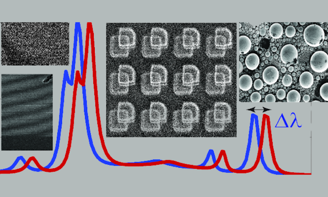
Properties and Characterization of Nanostructures:
The alluring properties exhibited through nanostructures are a manifestation of the quantum world's influence at the nanoscale. These properties transcend the area of classical physics, revealing a realm of magnificent behaviors. This phase ventures into the enchanting world of nanostructural properties and the strategies that unveil their mysteries.
Size-dependent Properties
As dimensions shrink to the nanoscale, the material's residences change dramatically. Nanoparticles' optical, magnetic, and electronic properties become to be size-dependent, allowing tailoring for specific applications. Gold nanoparticles, for an instance, showcase vibrant colors due to their plasmonic results.
Quantum Effects
Quantum confinement results dominate at the nanoscale, where electrons and different particles are restricted to discrete energy levels. Quantum dots exemplify this phenomenon, emitting different colors of light based on their size because of quantized energy levels.
Surface Area and Reactivity
Nanostructures' excessive surface area-to-volume ratio gives rise to more advantageous reactivity. Nanoporous substances provide substantial surface areas for catalytic reactions, gas adsorption, and drug delivery. This property has revolutionized fields from catalysis to environmental remediation.
Characterizing nanostructures
needs inventive tools and techniques. Scanning probe microscopy, transmission
electron microscopy, and X-ray spectroscopy get to the bottom of their shapes,
sizes, or even atomic structures. Properties like porosity and surface charge
are decoded through techniques like fuel adsorption and zeta capacity measurements.
Applications of Nanostructures:
The notable residences of nanostructures have paved the way for groundbreaking applications at some stage in a spectrum of industries. From revolutionizing electronics to redefining medicine, nanostructures have left an indelible mark on technology and innovation.
Electronics and Photonics
Electronics and photonics, the dynamic duo of modern era, find their prowess amplified by nanostructures. In the world of electronics, nanostructures like nanowires and quantum dots herald a brand-new generation of compact and power-efficient devices. Nanowires showcase exceptional conductivity, at the same time as quantum dots remove illuminated displays and solar cells with size-tunable colors. In photonics, nanostructured materials allow the manipulation of light on a nanoscale canvas, promising faster communication and more sensitive sensors.
Nanoelectronics:
Nanostructures have enabled the miniaturization of digital components, leading to faster and extra energy-efficient devices. Quantum dots and nanowires are integrated into transistors, creating high-overall performance processors and memory devices.
Optoelectronic Devices:
Nanostructures play a pivotal role in optoelectronics, where light and electricity have interaction. Quantum dots, due to their size-dependent emission, are used in LED displays and solar cells. Nanophotonics leverages nanostructures to control light on the nanoscale for improved sensing and conversation.
Medicine and Healthcare
Medicine and healthcare, beneficiaries of nanostructures' transformative touch, embrace revolutionary solutions that bridge the distance between technology fiction and reality. Nanostructures like nanoparticles and nanotubes function Trojan horses, delivering drugs with pinpoint accuracy to unique cells. These miniature automobiles preserve the promise of revolutionizing cancer treatments by way of minimizing side outcomes and enhancing therapeutic consequences. Additionally, nanostructured materials improve scientific imaging, illuminating the invisible and guiding precise surgical procedures.
Drug Delivery Systems:
Nanostructures offer specific manipulation over drug delivery, improving healing efficacy at the same time as minimizing facet consequences. Nanoparticles can encapsulate drugs, delivering them to specific cells or tissues. This focused approach is revolutionizing cancer treatment and different medical treatment options.
Nanomedicine Applications:
Nanostructures permit progressive diagnostic and imaging strategies. Quantum dots and nanoparticles enhance assessment in medical imaging, presenting clearer insights into disease progression. Additionally, nanostructured materials are used for tissue engineering and regenerative remedy.
Energy and Environment
Energy and the environment stand as beneficiaries of nanostructures' prowess, as these minuscule wonders open pathways to sustainable solutions. Nanostructured substances, such as those used in batteries and supercapacitors, bolster energy storage capacities, powering everything from smartphones to renewable electricity grids. In the world of the environment, nanostructures act as champions of purification, filtering pollution from water and air, or even catalyzing cleanser industrial strategies.
Nanomaterials for Energy Storage:
Nanostructures are using advancements in power storage technology. Nanostructured electrodes in batteries and supercapacitors offer higher strength and strength densities. This is critical for renewable power integration and the development of electrical motors.
Environmental Remediation:
Nanomaterials are harnessed for environmental cleanup. Nanostructures like nanoparticles and nanocomposites are used to remove pollutants from water and soil, addressing challenges in water purification and waste treatment.
Materials Science
Materials science, the realm of innovation at its middle, unearths its horizons increased by the influence of nanostructures. These architectural marvels bestow materials with extraordinary properties, reshaping industries and opportunities. Nanostructured materials, like nanocomposites, enhance mechanical power, electric conductivity, and thermal stability. These substances find their way into aerospace engineering, in which weight reduction is important, and construction, in which durability and sustainability intertwine.
Enhanced Material Properties:
Incorporating nanostructures enhances material properties. Nanocomposite materials showcase improved mechanical electricity, thermal stability, and electrical conductivity. These materials find applications in aerospace, automobile, and construction industries.
Nanocomposite Materials:
Nanocomposite materials, the fusion of nanoscale components with bulk materials, epitomize materials engineering's cutting-edge frontier. By integrating nanoparticles or nanofibers, these substances advantage greater mechanical, electrical, and thermal properties. Nanocomposites revolutionize industries which include aerospace, automotive, and production, paving the way for lighter, more potent, and greater durable structures and merchandise.
Nanostructures have converted
industries, sparking innovation and using development in ways previously idea
impossible. Yet, with their capability comes the obligation of addressing
challenges and looking forward to the future implications.
Challenges and Future Perspectives:
As we marvel at the accomplishments of nanostructures, we have to additionally apprehend the demanding situations that lie ahead. This realm of innovation isn't without its hurdles and ethical considerations. This phase delves into the demanding situations and provides a glimpse into what the destiny holds for nanostructures.
Scalability and Reproducibility
While nanostructures may be crafted with precision, upscaling production remains a assignment. Techniques that work in the lab might not translate without difficulty to mass manufacturing. Researchers try to broaden scalable approaches to meet the needs of the industry.
Safety and Ethical Considerations
As nanostructures grow to be integrated into regular products, questions get up approximately their impact on human health and the surroundings. Ensuring the safety of consumers and people and minimizing capability environmental harm is a concern. Ethical discussions also surround the capacity misuse of nanostructures in areas like surveillance and weaponry.
Integration into Existing Technologies
Integrating nanostructures into existing technologies requires overcoming compatibility issues and engineering answers for seamless integration. Collaborations among disciplines are essential to harnessing the whole ability of nanostructures in actual-world applications.
The future of nanostructures is
vibrant, with horizons that enlarge beyond our current creativeness. From
scientific breakthroughs to sustainable electricity solutions, nanostructures
are poised to shape the panorama of innovation for years to come.
Conclusion:
In this voyage through the sector of nanostructures, we have witnessed the transformative power of the small. From their humble beginnings in historical artisan practices to the forefront of scientific and technological development, nanostructures have unlocked doors to applications that regarded like magic only a few decades ago.
We've explored their numerous
sorts, fabrication strategies, extraordinary properties, and applications that
span from medicine to materials technology. Challenges had been acknowledged,
and the potential future landscape has been glimpsed. As we finish, let's
reflect on the importance of nanostructures in the tapestry of human
advancement and innovation.


0 Comments